

PCB and Electronics Testing Before and During Manufacturing: Importance, and Methods of Implementation


- What is the importance of electronics testing?
- 9 ways to check a circuit board
- MVI and AOI tests
- AXI test
- How to test PCBa board with ICT
- How to test a PCB board with FPT. Flying probe vs ICT
- How to check circuit boards with other PCB electrical tests
- Stress Tests
- How to test PCBs with FCT
- How to use other functional testing methods to check circuit board components
- PCB Lab Tests and Certification
- PCB simulations
- Сomponent tests with SPICE simulations
- Testing electronics with IBIS simulations
- Conclusion
The importance of electronics cannot be overemphasized. Our comfortable and stable existence to some extent depends on its reliability. In that regard, electronics testing gradually comes to the foreground. In this article, we will cover the most common PCB and electronics testing methods. As a company offering custom electronics design services, we are well familiar with many of these techniques and use some of them in-house.
- What is the importance of electronics testing?
- 9 ways to check a circuit board
- MVI and AOI tests
- AXI test
- How to test PCBa board with ICT
- How to test a PCB board with FPT. Flying probe vs ICT
- How to check circuit boards with other PCB electrical tests
- Stress Tests
- How to test PCBs with FCT
- How to use other functional testing methods to check circuit board components
- PCB Lab Tests and Certification
- PCB simulations
- Сomponent tests with SPICE simulations
- Testing electronics with IBIS simulations
- Conclusion
What is the importance of electronics testing?
Even carefully designed and well-made electronics are vulnerable to failure. Defects have to be identified before a device’s mass production, ideally at the development stage.
That is why it is so important to ensure adequate testing of electronics components, especially printed circuit board (PCB) testing.
Testing is a very important part of the PCB design process. When PCB testing continues throughout the production cycle, it helps to achieve economies and prevents or minimizes problems at the “end-of-the-pipeline” phase.
Before and during the manufacture of PCBs, a lot of designers’ efforts go into quality control and PCB testing. They have to be sure that a lot of indicators, such as current capacity, performance and impedance are within appropriate values, and the PCB has no short circuits, open or faulty solder joints.
There are many quality verifications to ensure high-quality designs are suitable for production at scale. Thus, Integra Sources’ designers first emphasize printed circuit board assemblies (PCBA’s) testing. Only then can they install PCBAs in a system and make a system-level test.
During manufacture and assembly, specialists conduct a series of printed circuit board tests. The purpose of PCB board testing is to rate a board’s yield and quality, and make sure the design was not damaged during assembly. These PCB checks are usually run on prototypes or small batches. They examine boards for probable electrical short circuits, imperfect solder joints, and test their functionality.
9 ways to check a circuit board
Various PCB analysis methods can be used for testing bare boards and assembled ones. Here are the foremost used approaches. They aim at checking the manufacturing process of a PCB and the quality of a PCBa.
MVI and AOI tests
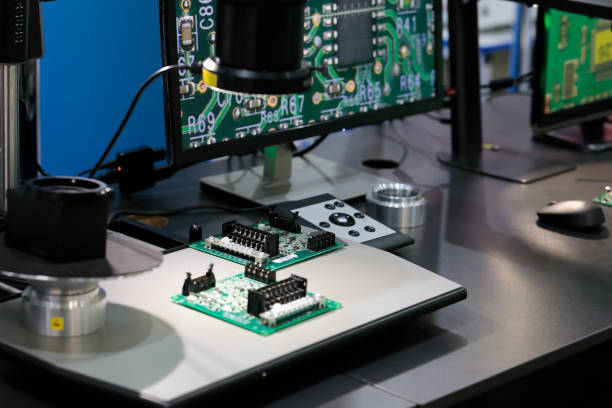
Manual visual inspection (MVI) was one of the first PCB testing methods applied to checking electronic circuits. As the name implies, the tester visually inspects a board to detect any shortcomings such as:
- poor solder;
- components absence;
- components incorrect orientation;
- broken joints;
- interrupted traces.
This method doesn’t suit mass production because of the growing PCB complexity and the high chance of human error. Still, it’s a viable technique in PCB design and prototyping.

Integra Sources’ team applies MVI testing to all printed circuit boards we work on, just in case. We partner with reliable vendors and always use high-quality components, so we detected faults with MVI only a few times. In one particular case, we noticed that diodes were placed incorrectly on the board. You can learn more about our projects on our portfolio page.
Although MVI may seem useless, it allows developers to detect and eliminate even slight flaws at early stages. That’s why Integra Sources applies this method to all PCBs we deal with.
Automated Optical Inspection (AOI) is the next level of MVI and a manufacturing test for large scale production.
AOI compares the images of your circuit test board taken by a single 2D or two 3D cameras to the image of an example.
This electronic testing equipment can be installed at the end of the production process, taking into consideration different manufacturing assembly methods. An AOI machine can be useful as
- the first step of assembly testing;
- for prompt reaction to the shortcomings.
It can also be combined with other methods of PCB checking, such as
- flying probes;
- in-circuit testing (ICT);
- functional testing.
AOI circuit board testing can help with a relatively large scale of production but is not suitable for work with prototype design.
AXI test
Automated X-ray Inspection (AXI) is a unique circuit board tester. By using X-rays, AXI creates 2D or 3D images of the hidden solder joints such as on Ball Grid Arrays (BGA) or Quad Flat No-leads (QFN) packages.
As one of the PCB testing services, it can be helpful
- in the volume manufacturing of PCBs;
- for complex boards;
- industrial PCBs’ production-testing.
The contractors that Integra Sources is dealing with make mandatory AXI tests to check the soldering and the absence of defects in the boards.
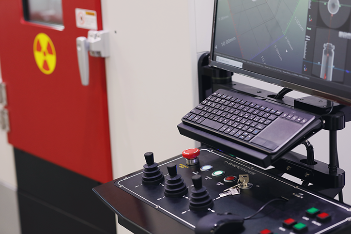
How to test PCBa board with ICT
In-circuit testing (ICT), also called the “bed of nails,” is an advanced PCBa component testing method. This printed circuit board testing technology is highly reliable but costly. Therefore, ICT is used in mass production as the concluding testing procedure for high-scale products.
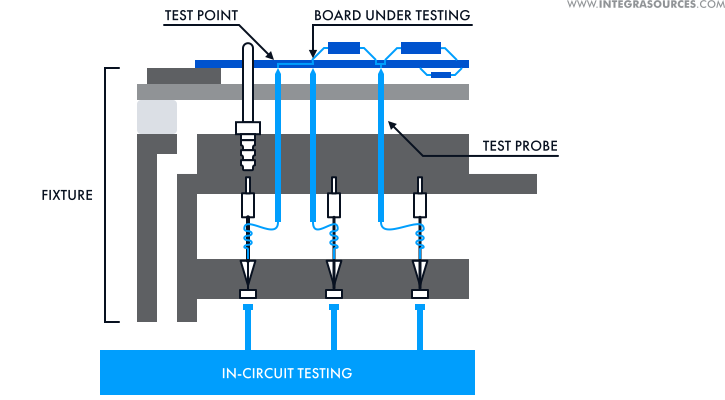
It’s a thorough component level testing technique that allows one to check a circuit board for shorts, opens, component orientation, resistance, and capacitance. ICT uses automated equipment and can detect about 90% of faults.
The tester has fixed sensor points (“nails”) placed in accordance with the design of the board. The sensor points check the integrity of the solder joints. ICT sensor probes link up with the PCB via relevant test points, making sure the connection is not damaged.
Large or follow-up batches can be checked with customized testing jigs or test fixtures, which provides cost-effective and prompt production lot testing. These printed circuit board testers can be
- mechanical (less expensive variant, needs an operator for manual actions);
- pneumatic.
PCB testing jig is great for
- dual-in-line (DIP)packages;
- pin grid arrays (PGA);
- PTHs.
In some cases, our clients ask to check components with the help of the PCB test fixture for automatic voltage measurement in PCB control points.
How to test a PCB board with FPT. Flying probe vs ICT
Flying probe electronics testing (FPT) is a less expensive type of ICT as it doesn’t need a test jig for PCB. FPT can be adjusted to a new PCBa easily but provides testing not as quickly as ICT.
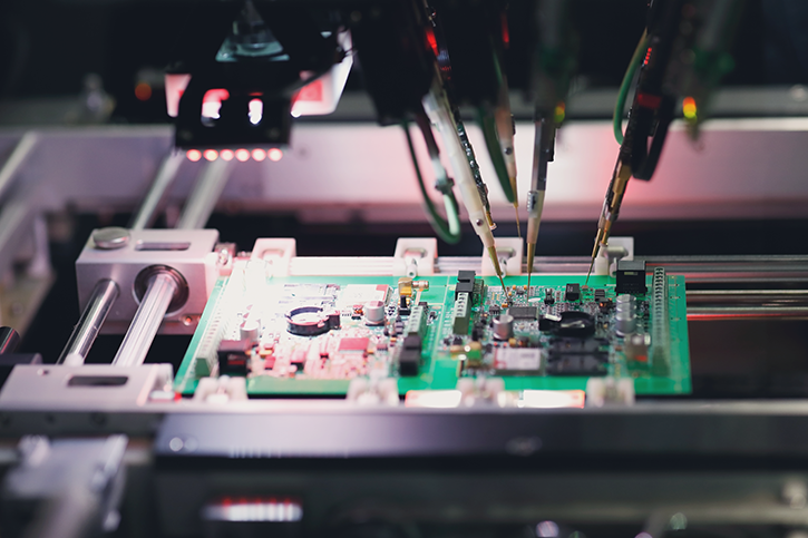
Unlike ICT, flying probe circuit board testing equipment uses several movable and fixed probes to contact:
- circuit board test points;
- the elements’ pads;
- unoccupied vias.
The movement pattern of the probe needles is customized for each PCB through programming, so no test fixture is required. This circuit board testing method is most suitable for
- prototypes;
- not large batch production;
- small-size multi-component PCBa.
Introduced in the late 1980s, this flexible PCBa tester has become popular among electrical component manufacturers.
How to check circuit boards with other PCB electrical tests
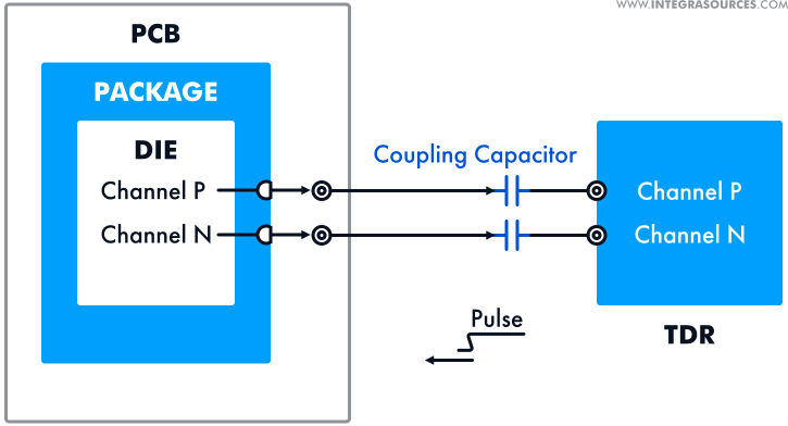
Time Domain Reflectometry (TDR) is electrical equipment for testing networks by measuring the reflections that appear from a signal going through a transmission environment. TDR is used as a PCB tester to find faults in high-frequency boards.
The Resistivity of Solvent Extract (ROSE) Testing – is one of the easiest and most reliable circuit board testing procedures in PCB and PCBa manufacturing. It can effectively analyze and identify any faults and significant surface residues remaining from manufacturing processes.
If a PCB is intended to operate in an environment where the risk of extreme electrical loads can take place, designers carry out appropriate testing of printed circuit boards. Electrical load tests can be performed as follows:
- Electrical Overstress (EOS) Tests allow one to measure the board’s resistance to overvoltage, overcurrent, and overpowering. The tests are performed at the wafer or individual device level. The board is exposed to overstress until failure, which allows for determining the maximum load the device can survive.
- Electrostatic Discharge (ESD) Tests are used to examine whether the board can survive an electrostatic discharge event, i.e. sudden electricity flows between two electrically charged surfaces. The surfaces build-up an electrical charge and then discharge it to the ground, impacting circuit boards and other electronic parts along the way.
There are three main models for ESD tests:
- The Human Body Model (HBM) simulates an electrostatic discharge delivered to the device from the fingertip of a standing person. This type of test uses an RC circuit to transmit an exponentially damped current pulse.

- The Charged Device Model (CDM) represents an ESD delivered from the device under test to another electrostatic discharge sensitive device with a lower potential. The CMD testing procedure involves placing a DUT on a test fixture, charging and then discharging it to an outside ground through a pin.

- The Machine Model (MM) represents a worst-case HBM event, or discharge coming from a charged machine into a grounded IC. For most use cases, this model is over severe. But such strong events do occur in real life, so the test can be useful for certain electronic devices.

- Environmental Stress Screening (ESS) Tests include various methods such as thermal cycling, drop testing, vibration testing, thermal or mechanical shock testing, and simulate other environmental influences that may affect the device during operation. Functional testing, which will be discussed below, is also performed alongside these tests to ensure design integrity and functionality. Since the tests evaluate the functionality of the printed circuit board under various stressful situations, they are usually performed by independent experts.
Integra Sources cooperates with responsible PCB manufacturers whom we trust to conduct mandatory tests. Nevertheless, based on the specific requests and needs of our clients, we can request additional checks or protocols of testing, for example, a protocol of manual board testing (as a rule, this is the measurement of voltages at the control points of the board).
Stress Tests
Other noteworthy methods are Stress Tests. They may be required to estimate the maximum allowable PCB limits within which it will remain functional and structurally intact. These tests don’t need to be used for all boards and very rarely on prototypes.
Design prototypes, as well as boards for large batch production, can be tested with Burn-in testing. This test is performed on the upper limits of PCB operating conditions such as temperature (257°F, or 125°C), frequency, or voltage to provide comprehensive information about the product’s reliability.

Stress tests belong to the HALT/HASS group of methods (Highly Accelerated Life Testing/Highly Accelerated Stress Screening) and are conducted according to HALT/HASS testing guidelines. These methods target the elimination of the identified shortcomings and to ensure product quality at the stage of development (HALT) or production (HASS). They are commonly used for
- new products that are introduced to the market;
- changes in a production procedure;
- high-reliability applications (aerospace, defense, medicine).
How to test PCBs with FCT
PCB Functional Tests (FCT) are aimed at checking if a board is working properly. These tests are used at the end of the manufacturing process, verifying a PCB’s functionality and its performance to specifications. Due to the design complexity and individual testing needs, PCBa functional testing can be either simple confirmation that the product will power up or a more complex investigation. A thorough production testing can be conducted according to requirements, protocols, or standards and includes software testing.
Functional testing is a must-have during small-batch manufacturing or prototyping when you need to be sure of the functionality of every PCB.
Preparation of functional testing has become a long and painstaking task due to the increasing complexity of devices.
By pre-production testing component elements of assemblies, manufacturers make it much easier.

How to use other functional testing methods to check circuit board components
Peel PCB tests measure the force needed to peel off a laminate in a PCB stack after it has been created and fully cured.
Solder pot and float tests determine the level of thermal stress a PCB plated through-hole (PTH) and via barrel can resist and their solderability.

Integra Sources design team carries out different types of FCT throughout each project. Our clients can be completely confident that both software and hardware involved in the project undergo complete testing to exclude even the slightest defects.
Thanks to well-organized quality control in production, we get boards without defects in 99.9% of cases. In a single case when the Bluetooth module’s contacts were not properly soldered, our specialists eliminated it on the spot.
PCB Lab Tests and Certification
You can entrust the testing of printed circuit boards to a specialized laboratory with various component testing equipment, and the ability to do PCB lab tests not only in the field of electronics but if needed, in physical and chemical fields for a comprehensive study of PCB’s safety and performance.
Labs are usually equipped with different electronic component testers, such as
- X-RAY inner layer registration tester;
- Plating thick tester;
- Impedance Tester;
- Copper Adhesion Tester;
- UV Spectrophotometer;
- other useful appliances.

An important aspect of the design of printed circuit boards is their compliance with certain standards and specifications.
These standards define some criteria that must be carried out on a designed board. You can read more about this in our article on PCB certification.
PCB simulations
Instead of physical tests of real boards, PCB pre-production simulation instruments can be used for calculating the electrical characteristics of the board. The choice of simulation is justified
- in the case of the high cost of instruments for measuring some characteristics,
- in the case of the necessity of making particular expensive PCB testing jigs.
PCB manufacturing expenses can be rather high, but so is the cost of possible PCB failure. Simulation allows designers to stay within a budget.
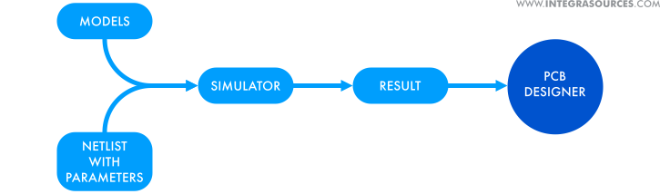
Any part of the printed circuit board can be analyzed. Simulation models can be used both for analog devices and for digital electronic components testing. PCB simulation software applies mathematical models to predict board operation.
Let us highlight some aspects and tools of this process.
Сomponent tests with SPICE simulations
Simulation Program with Integrated Circuit Emphasis (SPICE) is one of the most popular simulation tools used in PCB design testing.
Designers use SPICE applications for front-end engineering. These packages can perform different types of analyses, from the basic to the complicated ones. Each of them can help specialists to get useful data, for example, facts connected with component tolerances and sensitivities.
- DC Operating Point Analysis deals with static DC characteristics and calculates the circuit functioning under DC voltage. It is often the first phase of other analyses.
- DC Sweep Analysis computes the DC transfer curve, sweeping the DC values within a preselected diapason. It determines the required power supply and its limits, the current consumption, and allows engineers to be sure that all the circuit components work properly within their limits.
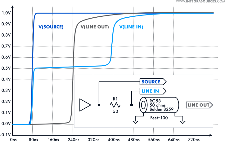
- The transient analysis is a timely response analysis. It calculates the voltage and current levels for predetermined time intervals and determines how the circuit will behave under mixed signals such as a big peak load or a peak change in the input. This type of analysis usually requires applying an oscilloscope to monitor waveforms.
- AC Analysis, or frequency sweep, deals with frequency characteristics and calculates the frequency response of the circuit. The AC analysis allows PCB designers to find out the behavior of the circuit when average AC signals are applied to its input.
Various business SPICE applications may contain different attributes, but they all have the same basic procedure for PCB analysis.
Testing electronics with IBIS simulations
Input/Output simulation has become a key element of digital system design at present. If problems connected with signal integrity are determined at the beginning of the design cycle, a developer can reduce the number of board fixes, and therefore, reduce the new PCB’s time of release.
SPICE simulators are commonly used in PCB design, but they have some drawbacks.
- They are a bit slow for transient simulation analysis.
- Not all of them are thoroughly compatible.
- Circuit board manufacturers do not want to share their SPICE simulations with the general public, as these models may contain intellectual property data.
Input/Output Buffer Information Specification (IBIS) for simulation of the integrated circuits’ input/output buffers is an alternative to SPICE simulation. Intel’s invention provides information about digital electronic components’ functionality and can be used during PCB development.
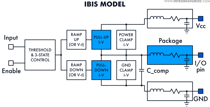
The advantage of IBIS models is that they can be applied to devices that haven’t got complete prototypes due to secrecy, complexity, or other reasons. IBIS was developed to provide consumers with precise IO buffer models without risking their intellectual property. So, the great advantage is that it can be a free electronic product testing method, as IBIS models for many devices are available over the net. The same electronic testing board may be used for the simulation of different constructors’ devices.
Conclusion
PCB design cannot be done without high-quality testing, especially when the complexity of products is increasing constantly. Choosing the appropriate test combination is usually a task of the PCB manufacturer, but very often outsourcing companies, which value their reputation and customers, conduct comprehensive PCB and PCBa tests. Electronic components testing can not only ensure the safety and reliability of the circuit board but in the long run, save time and money and increase the level of customer confidence by identifying and preventing potential defects before mass production.
Although Integra Sources relies on the experience and responsible attitude of our PCB vendors, we have highly skilled staff who constantly run various tests throughout the whole design process. We conduct both hardware and software-related tests and continue to stay in touch with clients after project completion.
You can also view an infographic variant of our post about PCB and electronics testing before and during manufacturing.
Related
materials
5 Common US & EU Consumer Electronics Certifications in Infographics
Certifying a product requires time and money, which is why making a mistake here can lead manufacturers to serious financial...
LEARN MORE 
LEARN MORE
Custom IP Camera for Monitoring Pets Remotely
The Wi-Fi camera allows people to see what their pets are doing at any moment. We provided PCB design and...
LEARN MORE
LEARN MORE

Guide to Consumer Electronics Certification in the US & EU: Requirements to Consider Before Mass Production
Although product certification takes place right before mass production, it is unwise to ignore the regulations during the development process....
LEARN MORE
LEARN MORE