


PCB Design and Layout Services

What we do


What’s included

Technical Specification

Schematic Design

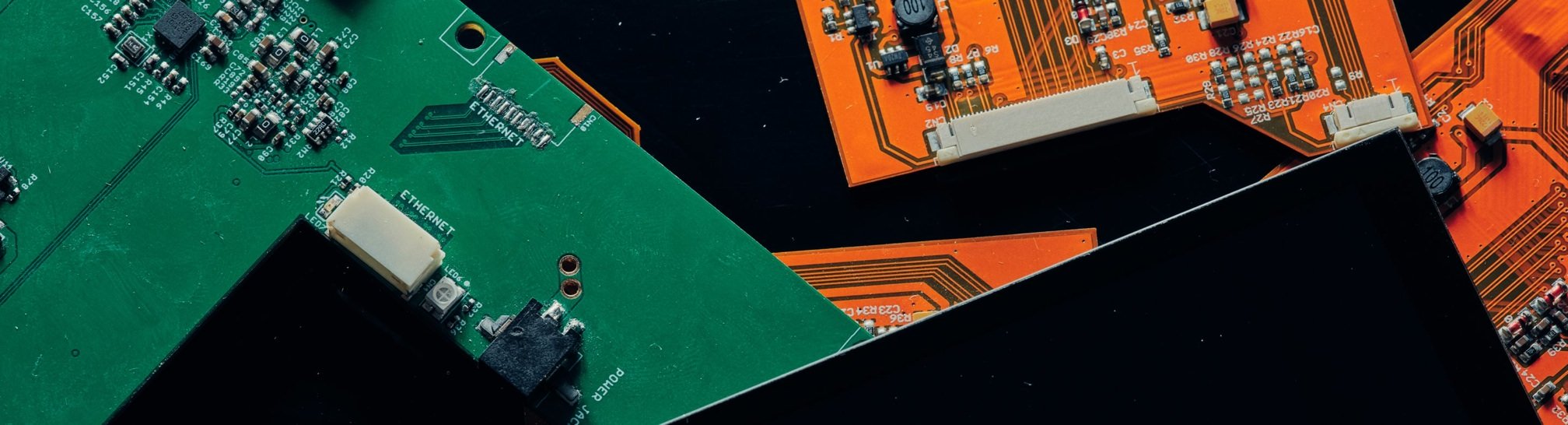
PCB Layout Services

Prototype Fabrication and Testing

Assistance with Mass Production

Warranty Period

Have an idea?
SUBMIT A PROJECT
Our projects

Vibration Conditioning Solution for Industrial Automation
Medical Alert Bracelet That Delivers Assistance at the Touch of a Button
A Control Panel for IoT-Based Smart Home Automation System
Awards


Why choose Integra Sources

Integration
- Adaptation to customers’ management systems
- Integration into customers’ development processes

Flexibility
- Flexibility in development
- Flexibility in communication

Communication
- High level of communication
- Personal account management
- Legal security guarantee

Transparency
- Transparency in development processes
- Customer’s dashboard
- Clear timelines
Industries
LEARN MORE ABOUT THE INDUSTRIES WE WORK WITH

Consumer Electronics

Power Electronics

Extractive Industry & Manufacturing

Healthcare

Logistics & Transportation

Science & Education

Agriculture

Entertainment

Robotics

Consumer Electronics

Power Electronics

Extractive Industry & Manufacturing

Healthcare

Logistics & Transportation

Science & Education

Agriculture

Entertainment

Robotics


Our tech stack
Processor Architectures
ECAD Software


Interfaces
Wireless Technologies


Math and Simulation Tools


Vendors


Testing and certification


Explore our workflow
GO to workflow page
We get acquainted with the concept of the future device and sign a non-disclosure agreement. The team gathers project requirements, studies relevant documents, and analyzes rival products on the market. At this phase, a preliminary project evaluation is made.
We contact the customer to confirm the project requirements. Then, we create a technical specification and set a budget and deadlines.
We make the final evaluation of the project, make up a team, and schedule its workload.
We sign a contract for custom PCB design services. The team gets to work.
We select components, design schematics and PCB layouts, and create one or more prototypes. The team identifies and eliminates bugs, and optimizes the performance of the devices. Customers receive daily reports on the progress. If necessary, the plan can be amended.
In parallel with hardware development or right after that, the team starts creating the firmware for the board. When the electronic circuit design is finished, we reveal and eliminate bugs and optimize the performance of the firmware.
The team tests the work of the board under corresponding operating conditions and runs some tests required for product certification. If necessary, the PCB is then modified.
After the tests, we finalize the documentation necessary for mass manufacturing, including the bill of materials, Gerber files, etc. If necessary, Integra can also help you choose a manufacturer. We can also prepare manuals if the product is designed for in-house use.
The product is handed over to the customer. A free warranty period starts. During this time, the team will fix any bugs and defects in the product.
Reviews


Frequently Asked Questions
What do I get when the project is finished?

Do you do receipt inspections of the components you receive?
What about intellectual property rights?
What technologies do you use for PCB design and layout?
Can you build a device prototype?
How many layers can I get on a PCB board?
Do you validate PCB layouts before production?
Can you estimate the cost of the final device before it's built?
Can you guarantee the quality of the product?
Can you help me with certification?
What is the minimum completion time?
Can you help me with enclosure design?
Who are your customers?


Related services

Firmware Development Services
As a firmware development company, we have extensive experience with hardware, operating systems, low-level diagnostic and performance tools.
LEARN MORE 
LEARN MORE

Board Support Package (BSP) Development
As part of our BSP development services, we create low-level operating system code, device driver code, and other files with...
LEARN MORE
LEARN MORE

Embedded Linux Development Services
Integra has vast experience with various Linux distros and offers various embedded Linux development services. We can build, customize, and...
LEARN MORE
LEARN MORE