

High Speed Printed Circuit Board (PCB) Design Guidelines


- What Is High Speed Board Design?
- What Boards are Considered High Speed?
- High Speed PCB Design Rules and Challenges
- Trace length tuning
- Impedance
- Track shape
- Termination
- Grounding
- Components location
- Placement of ground polygons on the layers close to the signal layers
- Crosstalk
- Tips for High Speed PCB Design: First-Hand Experience
- CAD Software Helpful Features
- Final Thoughts
To get a brief idea of high speed PCB design, you should take a look inside an electronic device. If it works at high frequency and uses a high speed interface — then it is more likely that its PCB is high speed. In this article, we will provide high speed layout guidelines including design rules and handy tips based on our personal experience.
- What Is High Speed Board Design?
- What Boards are Considered High Speed?
- High Speed PCB Design Rules and Challenges
- Trace length tuning
- Impedance
- Track shape
- Termination
- Grounding
- Components location
- Placement of ground polygons on the layers close to the signal layers
- Crosstalk
- Tips for High Speed PCB Design: First-Hand Experience
- CAD Software Helpful Features
- Final Thoughts
Nowadays, a printed circuit board of any modern electronic device should meet the requirements of technologically advanced solutions. That is why high speed and high frequency PCB design has become a hot topic for hardware engineering professionals.
The market for electronic devices is tremendous. Suffice it to say that the high-tech medical device market alone is projected to quadruple in five years to reach $264.8 billion by 2028.
That is why it is really important for every PCB designer to know high speed board design basics. If you are in the loop already, go ahead, take a shot and design a high speed PCB. Doing this, you will get the necessary skills and experience, uplevel yourself, and stay a go-to engineer.
Our team has already had such experience performing on high speed PCB design projects. So we decided to write this article to underscore the relevance of its topic and share our personal experience.
We hope our high speed design guidelines supported by first-hand recommendations will be helpful to designers who make their first steps in exploring this area.
What Is High Speed Board Design?
As the name suggests, a high speed printed circuit board design provides the transmission of signals at high speeds. In other words, a device with a high speed design PCB can transfer data at a very high rate. This capability opens up a lot of opportunities for engineers and manufacturers, helping them create the most advanced electronic solutions.
With that, it raises certain difficulties at the development stage that mostly relate to the integrity of signals propagating across the board. You can relieve the integrity issues by choosing the right PCB material, but you can still face some serious challenges, including:
- electromagnetic interference (EMI);
- signal propagation delays;
- crosstalk;
- signal degradation.
The generally accepted PCB design standards will not always work here. There are special high speed PCB layout techniques that can simplify the design process and help you avoid potential issues. We’ll talk about these techniques later in the article, but first of all, let’s point out the main features typical of a high speed PCB.
What Boards are Considered High Speed?
You can identify a high speed PCB design by certain characteristics. So, the design is high speed if:
- it uses HDMI, Ethernet, SATA, PCI Express, USB, Thunderbolt, or other high speed interfaces for the fast data transfer;
- the circuit consists of several sub-circuits connected to each other through high speed interfaces (LVDS, DSI, CSI, SDIO, DDR3, etc.);
- the time of signal propagation over the track is at least ⅓ of the signal rise time;
- the digital signal frequency is of 50MHz and over;
- the size of the printed circuit board is very small, and the location of the components becomes a real challenge (especially when you come across a high speed interface layout).
To sum up, high speed PCB design is applied to devices with PCBs working at high frequencies with the use of high speed interfaces. With that, the amount of data and speed of its transfer mean the world.

This picture illustrates a part of high speed PCB design developed by our engineers for a home automation system. Our team managed to meet all the challenges and achieved great results in the development of a tablet-style smart home head unit.
High Speed PCB Design Rules and Challenges
As in every engineering process, there are certain rules and directions on how to design a high speed PCB schematic and layout. Let us consider the key points and challenges which may arise at the same time.
Trace length tuning
When you use a high speed interface, you need to tune the length of the traces to synchronize signal propagation through data lines. If it is not synchronized, the interface could fail at the maximum frequency or will not work at all. That is why tuning the trace length is a critical aspect in a high speed design.
The higher the interface frequency, the higher the requirements of the length matching. As you know, there are two types of interfaces in PCB design and length tuning will be different for each of them. For a parallel interface, we tune only the lengths of the traces. The main challenge is that there are many traces with a lack of space for length tuning. For a serial interface, we unite signals into several differential pairs.
Length matching rules for differential pairs are more complicated. All traces should have the same length with a tolerance of X mm. With that, the length of the traces should be equal in each pair with a tolerance of Y mm, given that Y < X.
Aligning of the traces’ lengths leads to the loss of the distance equality between the tracks of a differential pair. You should make sure that the length of such equality-loss regions is not more than the maximum uncoupled length.
For extremely high speed interfaces, it is important to remember about the interconnecting delays inside CPUs, FPGAs, etc. Bear these delays in mind when you tune the tracks’ length.
Modern CADs have built-in tools for trace length tuning. Before you start using such tools, you should define aligning rules for each of the interfaces. It is important to know which particular rules and limitations you should define.


Impedance
When you make a PCB layout or a high speed PCB layout, you should observe single-ended impedance Zo as well as differential impedance Zdiff.
Zdiff, recall, is the impedance between two coupled tracks, aka a differential pair. Characteristic Zo is the impedance of single lines that are not united into differential pairs.
There are typical impedance values for each interface both parallel and serial.
There are also other types of impedance:
- The odd-mode Zoo value is affected by the capacitance and inductance between the two traces and Common Zcm is defined as an impedance that occurs when testing a pair of lines driven by identical signals.
- Common Zcm is defined as an impedance that occurs when testing a pair of lines driven by identical signals.
- Even mode Zoe is the impedance measured while testing a single transmission line of a pair of lines that are driven by identical signals with the same amplitude and polarity. The even-mode value is twice the common-mode value.
Although one rarely faces these impedances, they should still be taken into account. The wrong single-ended or differential impedance causes signal reflections in the track. This will, in turn, decrease the signal quality, lower the working frequency, and generate electromagnetic interference.
Therefore, keeping impedances at the right level is one of the key rules of high speed PCB design.

Track shape
Developers rarely use straight tracks from sources to receivers on PCBs, especially when dealing with high speed interfaces. Bending tracks is a common way of tuning track lengths.
Ideally, you want to use smooth rounded corners, but this technique requires too much time.
Moreover, when optimizing the layout, you need to redraw each track a few times, which makes such a design even more time-consuming.
What engineers never do is bend tracks at 90-degree angles. At such bends, the track becomes way too wide, which changes the impedance in this section of the track and causes reflections. In the case of differential pairs, this also leads to a higher value of uncoupled length.
That’s why the best practice is to use 45-degree angles.

Termination
Termination prevents reflections caused by impedance mismatches. The termination process involves placing elements (usually resistors) along the PCB so that the high-speed signal has the same impedance throughout the line path.
Today the most common type of termination is parallel termination. The idea is to place a resistor between the tracks of a differential pair at the end of the line, as close to the receiver as possible.
Termination makes it possible to effectively get rid of signal reflections in the tracks, therefore, upgrading the quality of data transfer. In the case of differential pairs, the resistor value should be equal or a little more than Zdiff.
The low value of the resistor will cause over-termination which will adversely impact the signal quality.
Some ICs have termination resistors inside. In this case, you do not need external resistors because they will cause over-termination. That’s why it is important to learn datasheets and hardware design guides for all ICs you use.

Grounding
In most cases, you cannot trace high speed interfaces on one layer. Thus you need to move traces to the other layers with the help of vias. Vias are electroplated holes through which traces can connect with each other on different board layers.
GND polygons potential on different layers should be the same near signal vias. That's why you should place GND vias as close to them as possible. Such GND vias are called stitching vias. This approach allows keeping the same GND reference all along the high speed trace.
Vias used for high-speed signal routing should have enough space between them. Otherwise, densely populated vias can lead to high current density and eventually overheating.
The improper design of vias can cause impedance discontinuities. To avoid this, all vias should have an appropriate diameter either on the board layout or on the manufactured PCB.

Components location
Another portion of important high speed PCB layout rules deals with component placement. Before beginning, we recommend that you map out the location of components on the board.
One particular way is to sort them out based on their functions. If they perform similar functions or participate in the same process, we recommend grouping them close to each other.
If the board has analog components, they should have their own GND polygon. To avoid EMI, they should also be located away from digital components and traces.
When placing high speed components on the board, keep in mind that the traces are quite short. Make sure there’s enough space for length tuning. Avoid locating them too close to interference sources (for instance, switching power converters).
Also, do not place high speed interfaces close to the PCB edges because this will reduce the signal quality. The common practice is to group such components at the center while leaving the connectors at the edges of the board.
The components’ location becomes a real challenge when a PCB is of a very small size. Following the location rules for high speed design, we placed the components in the most accurate manner on a small PCB for a custom IP camera.

Placement of ground polygons on the layers close to the signal layers
You should route tracks of high speed interfaces over a solid GND plane.
We do not recommend you route tracks over cutouts in polygons or over polygon-splits. Otherwise, you will get extra EMI, signal propagation delays, integrity violation, generation of interference and finally, degradation of the signal quality.
If the tracks happen to cross polygon-splits, it is necessary to place ceramic stitching capacitors at the place of polygons splitting. This will minimize the negative impact on the signal.

Crosstalk
Crosstalk occurs when a signal transmitted on one track causes an undesired effect on another one, usually the neighboring track. Crosstalk manifests itself as a change in the signal.
The strength of crosstalk is related to the length of the section where neighboring tracks run parallel with each other. The longer the section, the stronger the effect.
Adhere to the 3W rule to minimize crosstalk: keep the distance between the tracks at least three times longer than the tracks’ width.
In the case of differential pairs, the distance should be at least five times longer than the track’s width. This is called the 5W rule. The same distance should be kept between differential pairs and other neighboring tracks.
If a differential pair serves to transmit a periodic signal, e.g. clocking, we recommend you increase the distance from this differential pair to the other differential pairs or any other tracks up to 8-10W.
Pay special attention to the tracks of asynchronous signals (enable, interrupt, reset, etc.). You should make the distance between these tracks and tracks with high speed signals as long as possible.
Sometimes we use two neighboring layers in a multilayer printed circuit board to route signals. Doing this, remember to route the tracks on one layer perpendicular to the tracks on the second layer. Thus you will avoid parallelism of the tracks and minimize crosstalk between them.

We have mentioned the basic high speed PCB board design rules but not all of them. This is a wide area of an even much wider area called PCB design.
In its turn, PCB design is a part of such a vast and multistage domain as embedded hardware development. It includes, for instance, preparation for production and selection of components. At these stages, one should consider a million nuances, such as the device production time, the scheduled time for discontinued components, and whatnot.
We can take care of all the details delivering your project as part of embedded hardware design and development services that we provide.
Tips for High Speed PCB Design: First-Hand Experience
As a team of developers who have been adept at high speed PCB design, we`ll be happy to share our experience with you. So here are some first-hand tips that you can use to streamline your workflow while designing a board with high speed signals.
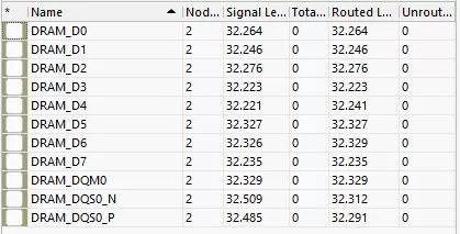
As mentioned previously, tuning of traces’ length is a crucial aspect in high speed design. The main problem is that the built-in tools of modern CADs allow controlling the overall length of the traces.
However, if the tracks of a high speed interface pass on several layers, you should align both the overall length of the traces and sections of the tracks on each layer. The reason for this is that signal propagation time is different on different layers.
To control the section lengths, it is easy to use an excel or google spreadsheet. You should add the lengths of the track sections located on different layers. Although you add data manually, this approach helps you tune the trace length with the required accuracy.
Another important aspect that we mentioned above is an impedance issue. Our strong recommendation, or even a must-do, here is to ask your manufacturer about their PCB stacks and parameters of the tracks. You need this to get the required impedance on different layers.
This is really essential because calculated values can differ from the actual impedance. Depending on each manufacturer, there is a slight difference in the characteristics of materials that affect impedance.
Before you set the design rules of high speed interfaces on your board, you should choose the right manufacturer and check all the details. Ask them about the stack-up options they have for the number of layers you need. Learn about the length of the tracks and distance between them to obtain the required single-ended and differential impedance.
Get information about the length of the tracks and distance between them to obtain the required characteristic and differential impedance.
To get the needed impedance of some tracks on manufactured boards, you should indicate these tracks on the design.

Don’t forget to ask your manufacturer to perform the impedance control procedure. Such a procedure will add to the cost of manufacturing but will allow the designer to increase the quality of high speed signals on the PCB.
It is always very useful to get new knowledge and adopt experience from other developers for both newcomers and advanced engineers. Our engineers are no exception. They are constantly trying to replenish their store of knowledge and move with the times.
One of the most efficient methods of doing that is to take various courses and training programs.
Integra Sources' developers regularly replenish their knowledge through courses provided by reputable educational institutes. For example, training at FEDEVEL Academy gives helpful information regarding high-speed PCB layout. From our personal experience, we would recommend the Advanced PCB Layout Course by FEDEVEL Academy. They provide high speed PCB layout guidelines that will help you improve yourself.

For newcomers, this course can help teach how to start, what to do first, what to do next, how to check every part of the PCB, how to create output documentation, and a lot of other information. Experienced engineers will be able to learn a lot of useful PCB design tips and tricks which can save plenty of time.
CAD Software Helpful Features
One more helpful tool that can leverage your high speed PCB design is your CAD software. We at Integra Sources are able to use Altium Designer, EAGLE, Cadence Allegro, KiCad, and others. The functionality of Altium Designer facilitates a high speed layout design to a large extent. We would like to show you some useful features of this tool.
Propagation Delay is an Altium function which is very helpful for high speed PCB design. This function allows a designer to see the length of the signal traces and the signal propagation delay at the same time.
The Propagation Delay feature can be really handy in the places where you need a certain signal delay on a specific track. You can also set a rule in the Design Rule Check (DRC) to check that the selected tracks meet the preset conditions, for example, to minimize the delay difference between differential pairs.

The screenshot above shows how the rule in the DRC works. We set an acceptable propagation value and after the rules are checked, a mismatched track is detected.
Another useful feature of Altium Designer is Interactive Sliding. This function tackles a number of issues that you might face during high speed layout. The picture below shows a preferred way to lay out a BGA microcontroller.

Interactive Sliding assists greatly in the design of non-standard printed circuit boards, such as ring-shaped PCBs.

Impedance Profile is another useful tool that allows developers to automate track impedance and width calculation. Target impedance is set in the Impedance tab of the Layer Stack Manager of Altium Designer. Based on this and other parameters, as well as the stackup used in the project, the program calculates the track width on a specific layer required to deliver the target impedance.

Altium has a wide range of interesting features including their collaboration with GitLab and SolidWorks.
You can look through all GitLab threads, track the detailed change history, and push changes directly from Altium.
SolidWorks Collaboration makes it possible to edit a board straight in SolidWorks. You open a 3D model, place the components, save changes, and then just edit the tracks in Altium.
Final Thoughts
As you can see, high-speed design is a complex but fascinating subject that leaves plenty of room for research and practice and is much sought after today. The PCB designer needs to always stay on topic to meet the needs of the age.
If you need assistance with high-speed PCB and system design or a professional review of your existing design, you are always welcome to contact us with your inquiries. Our experts are ready to share their experience and help you meet your needs for PCB design and layout services.
Related
materials


Customizable Capacitive Keyboard
Integra Sources created a highly customizable keyboard that meets all modern requirements and will appeal to the fans of exclusive...
LEARN MORE 
LEARN MORE

PCB and Electronic Testing Methods in Infographics
Discover various PCB testing methods needed to ensure the quality and functionality of electronic devices.
LEARN MORE
LEARN MORE
PCB and Electronics Testing Before and During Manufacturing: Importance, and Methods of Implementation
Find out how PCB designers and manufacturers test circuit boards before and during production and why these actions are so...
LEARN MORE
LEARN MORE