


This website uses cookies so that we can provide you with the best user experience possible. Cookie information is stored in your browser and performs functions such as recognising you when you return to our website and helping our team to understand which sections of the website you find most interesting and useful.
Electronics Design Practices to Prevent EOS and ESD Damage
July 15, 2022 20 min read
last update: January 15, 2025


Contents
A simple touch can actually destroy or seriously damage an electrical device. Many objects, including the human body, can accumulate static electricity. By touching the external connectors of a device, one can damage its sensitive integrated circuit. The voltage of such charges can reach several thousand volts, which is deadly to sensitive components. Protecting devices from such events is an important challenge for electronics developers.
In this article, we will discuss the sources and nature of electrostatic discharge events and electrical overstress. We will also talk about ESD and EOS failures, as well as the methods of EOS and ESD protection.
What is ESD?
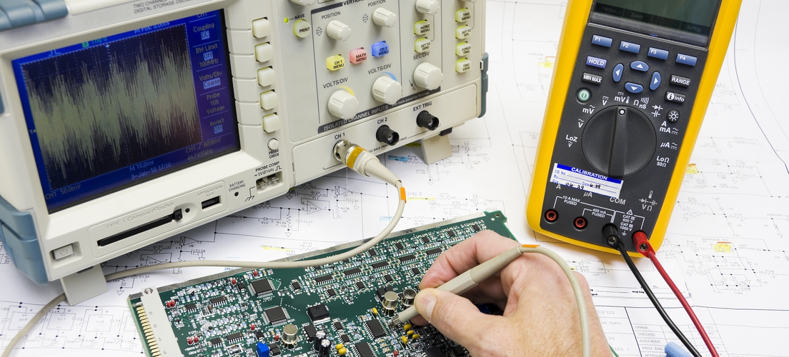
Our team has vast experience in developing custom electronics, so we know very well how problematic ESD can be.
ESD stands for electrostatic discharge. Many materials can conduct electricity and accumulate an electric charge. It happens due to triboelectric charging (friction between materials) or electrostatic induction. Whenever this happens, an object builds up a stationary charge (static electricity) on its surface. When this object is placed too close to another electrically charged object or material, the voltage difference causes the electric current to flow between them until the charge balance is restored.
Thus, one can define electrostatic discharge as a momentary electric current flow between two electrically charged materials or objects which is caused by contact, an electrical short, or dielectric breakdown.
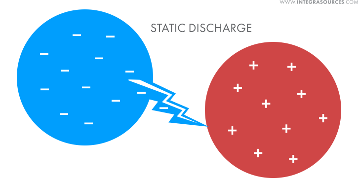
Static electricity may seem like an everyday occurrence. But the voltage of an electrostatic charge can reach several thousand volts, which is a serious hazard to components. In modern microelectronics, everything is becoming smaller and thinner, which leads to high ESD sensitivity. As a result, even an overvoltage of 10V can damage integrated circuits. For comparison, when a person walks over a carpet, the static potential on his shoes can reach 35,000V.
Electrostatic discharge events threaten electronic devices both during the production phase and during operation. According to EOS/ESD Association, inc., the damage caused by such an event can cost between a few cents and several hundred dollars per device. In the case of mass production, a whole production batch can be regarded as defective. And that’s thousands and millions of dollars.
That’s why we take EOS and ESD protection seriously when developing electrical devices for our customers. Check our electronics design services to learn how our team can help your project.
ESD vs EOS
Electrical overstress is another phenomenon similar to electrostatic discharge. In fact, engineers often use these terms interchangeably. Both these events can be defined as the exposure of an electrical device or its components to a current or voltage that exceeds the device’s maximum ratings. However, they are slightly different.
An ESD event:
- lasts for a very short time (nanoseconds);
- features a moderate peak current;
- and reaches extremely high voltages (up to several kilovolts).
An EOS event:
- lasts for a longer time (milliseconds and sometimes even seconds);
- features a higher peak current;
- but reaches lower voltages (up to dozens or hundreds of volts).

EOS can have many different sources, such as excessive currents or voltages, power-on/off transients, etc., while the sources of ESD are electrostatic only. From this perspective, electrostatic discharge events can be regarded as a subset of electrical overstress.
Imagine a device plugged into a 110V socket. If lightning strikes the electric substation powering this socket, the device will receive 400V for a few milliseconds. That’s an EOS event. If a person is trying to plug a USB cable into his smartphone and an electrostatic charge (from his body or clothes) strikes the USB port, the port will receive 1,500V instead of the standard 5V. That’s an ESD event.
What Damage Can Electrostatic Discharge Do to Electronics?
A powerful electrostatic discharge can cause various failures. The ESD damages and their severity depends on several factors, one of which is how the charge is dissipated to the topology of the integrated circuit.
When an electrostatic discharge event occurs, the static charge (that reaches very high voltages) causes a high peak current. Although the event lasts for a very short time, it is often enough to cause burnout if the device is not properly protected. The amount of heat generated during the event is enough to fuse the interconnecting links wires or the components in the chip.
Sometimes, components or connections are not destroyed completely. In such cases, the IC will still function with no noticeable performance drop. Sometimes, a partially damaged IC will continue working, but its performance will slightly drop. It often happens to analog devices.
In other cases, this event can cause damage due to overvoltage rather than heat. High voltages can breakdown insulating oxide layers. It can either destroy the IC completely or do partial damage to it with no noticeable performance drop.

Disregarding these dangers can lead to costly consequences. Feel free to contact our team to discuss how we can minimize such risks.
The consequences of an ESD event can be divided into four types.
- Soft failure
In this case, the event causes no physical damage to the IC. Instead, it causes the system to malfunction or stop working. Nevertheless, such failures can be corrected in the system, or you may simply need to reboot it.
- Data loss
In some cases, the event doesn’t cause physical damage but corrupts data, software, or firmware installed on the device. For example, if lightning strikes too close to a house, it can result in full data loss on the hard drive of the personal computer in the house.
- Catastrophic failure
A catastrophic failure is permanent damage that disrupts the work of the device completely. It happens when an electrostatic charge melts metal, breakdowns junctions or insulating oxide layers.
- Latent defects
As mentioned above, an electrostatic discharge can cause a partial degradation of the IC, but it will continue working. This damage type is referred to as latent defects. On the one hand, such defects are not critical. On the other hand, detecting them is very difficult. Moreover, sooner or later, these defects will lead to critical failures. Some manufacturers are known for producing low-reliability devices and equipment. Often, it happens due to poor antistatic protection used at the plant, which leads to frequent ESD events and latent defects.
Devices can be classified by their ESD immunity level. ESD Association 2.0 Handbook is used for defining a device’s ESD performance in manufacturing environments. But for real-life situations, developers commonly refer to the IEC 61000-4-2 standard which defines four standard ESD circuit protection levels. You can read about this and other PCB and electronics testing methods in one of our previous articles.
Common ESD protection methods
Since electrostatics discharges can be deadly to electrical devices, it is not surprising that combating ESD in electronics is vital for their nominal operation.
Certain protection measures can work for electrical overstress as well. For example, according to Osram Licht AG, LEDs and other electronic components can be protected with overvoltage protection devices and current limiters (TVS diodes, fuses, etc.). Nevertheless, such measures are usually not effective in preventing EOS damage. Although ESD and EOS are similar in nature and consequences, the reasons causing them are different.
EOS is regarded as an unlikely event which should not happen under normal operating conditions. Most EOS protective measures are taken at the design phase: by designing the device with a higher Absolute Maximum Rating. It will make the device less vulnerable to electrical overstress but will not protect it if the voltage/current exceeds these limits.
As for ESD protection, three groups of measures can be used.
Protected Working Area & ESD-Control Tools
The first thing one should do to protect a device from static electricity is to establish an ESD-Protected Area. In an EPA, all objects, surfaces, people, and devices are linked to ground. This way, their potentials are kept at the same level. Creating such areas is the first line of defense against ESD in electronics manufacturing.
The basic elements of such areas are: an antistatic mat (1), ground cable (2), grounding plug (3), ESD loop (4), and ESD wrist strap (5).
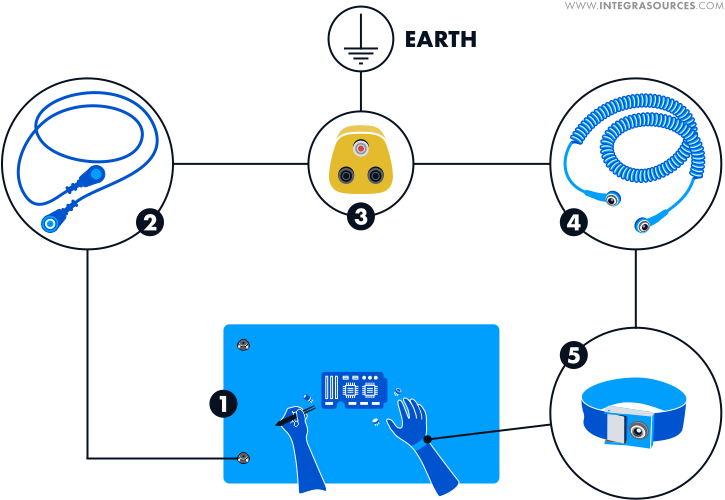
This is the simplest EPA one can build to provide a minimum level of protection. But if there’s a need to minimize the risk even further, one can build much larger and more complicated ESD-protection areas. Engineers can also use a variety of additional tools and devices designed for coping with ESD in electronics.
Ionizers are filtration and recirculation devices that generate positive and negative ions around the sensitive equipment you want to protect. This reduces the chances of an ESD event. They also remove airborne particulates that can cause friction and static charge build-up.
ESD test equipment is used to measure the level of electrostatic discharge for a particular object, surface, or person. This way, one can make sure the ESD stays within acceptable levels.
Antistatic bags and ESD packaging boxes are used to store PCBs or devices. They don’t allow static electricity to build up, providing constant protection.
Electronics designers can also use antistatic gloves, shoes, ESD-safe tools, ESD tape, and other equipment and tools.
A properly organized EPA will protect electronics from electrostatic discharge events during the working process. But engineers should also ensure the device will not suffer electrostatic discharge events while in operation. One of the ways to do it is to use overvoltage protection devices.
Mounting Overvoltage Protection Devices on the PCB
Electronics designers have to provide proper protection from various situations: lightning strikes that induce high-voltage spikes, transients that cause overvoltage, and electrostatic discharges. Voltage limiters can prevent dielectric breakdowns.
There are many types of overvoltage protection devices, including ESD suppressors, varistors, Zener diodes, and similar components. But most commonly, engineers use transient voltage suppressor (TVS) diodes. That’s why we often use TVS diodes in custom electronics design as well.
TVS diodes are placed in parallel with the circuit that requires protection. Under normal conditions, a TVS has a very high resistance. Therefore, the current doesn’t flow through it. However, when the induced voltage exceeds the avalanche breakdown voltage, the diode’s resistance drops. As a result, it shunts the excess energy generated by the overvoltage event to ground, not allowing the current to flow to the integrated circuit under protection. When the voltage drops to the normal level, the diode resets.
The following scheme explains how the ESD current flows through the TVS diode array to ground.

ESD protection devices must be placed at all external connections and sometimes on human input devices (for example, keyboard keys or buttons). These are the “gaps” through which static electricity can enter the circuit.
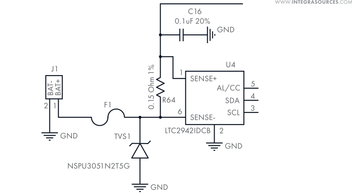
One of the projects our team worked on was a medical device with multiple external connections. The team had to protect all of them.
In the scheme below, you can see a TVS diode placed in parallel with the protected circuit after a battery connector. The team used the NSPU3051N2T5G unidirectional ESD and surge protection device here. It protects the circuit from possible electrostatic discharges that can be generated by the human body or clothes when a person replaces the battery. If an ESD event occurs, the diode will shunt the excess voltage to ground, not letting the current flow to the circuit.
Another TVS diode was placed at the USB port of the device. The capacitors here protect the circuit from low-frequency EMI and play no role in ESD protection. Usually, USB ports are protected with specialized TVS diode arrays – for example, D3V3F4U6S-7. But in this case, one TVS was enough.

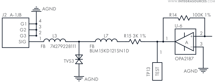
The medical device also had several connectors for ECG electrodes which can be the sources of static electricity too. Note that the U6 operational amplifier used in this scheme has an output pin (1) with very low resistance. It means that the amplifier can work as another TVS diode. For that reason, the circuit is also protected with a resistor (R15) that reduces the residual pulses that were not stopped by the TVS protection.
Sometimes, it’s impractical to protect each and every connection of your device. When our team developed the PBX Communications Device for Preventing Phone Fraud for Senior Citizens, we decided to leave most of its connectors unprotected. First off, the customer wanted to reduce the cost of the device as much as possible. Second, considering how the device was supposed to be used, the team didn’t expect electrostatic discharges to be serious hazards.
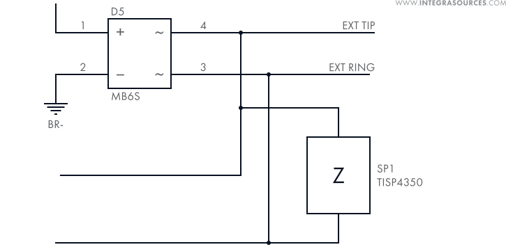
Therefore, we provided protection only for the telephone line. Instead of a TVS diode, we used a TISP4350 overvoltage protector: this series was designed specifically for overvoltages on telecom lines.
The choice of protection device depends on a number of factors. Different models and types are designed for different voltage ranges, working voltages, event duration, response time, etc. Naturally, an electronics designer chooses components with these parameters in mind.
Size is another important metric, as large components cannot be used in small devices. And of course, our team takes into account prices and availability as well.
ESD Protection Circuit Design
When it comes to protecting sensitive circuits from ESD, design is another effective tool that works in tandem with ESD protection devices. Electrostatic discharge protection is based on the TVS’ ability to shut electrostatic current to ground. Therefore, when designing a PCB, ESD protection can be achieved if the path to ground has as low impedance as possible. As experts in PCB design and layout, we use these and other design techniques for ESD protection.
1. Optimizing impedances around the TVS
All PCB components and traces have parasitic inductances. In a typical protection scheme, there are four of them: the inductance between the ESD Source and the TVS array (L1 and L2), the inductance between the TVS and ground (L3), and the inductance between the TVS and the protected integrated circuit (L4). ESD current can be forced to ground only if L4 is larger than L1-3.

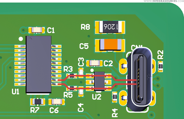
The picture below shows the PCB layout we designed for one of our projects. As you can see, this part of the board has a USB port. To protect the FT231X UART (U1), we placed a USBLC6-4SC6 ESD suppressor (U2) on the path between it and the port.

There are two things worth noticing here.
- The suppressor (U2) is placed closer to the ESD Source (USB port). As a result, the inductance L4 becomes much larger than L1, which forces possible ESD current to the TVS.
- The suppressor is placed directly on the path from the ESD Source to the Protected IC, which completely removes L2.
2. Limiting EMI from electrostatic discharge
An electrostatic discharge is a fast transient that causes electromagnetic interference. An electrostatic discharge event generates a rapidly changing electric field that can couple onto the nearby circuits. It can cause undesired voltages on unintended circuits. The traces between the ESD Source and the TVS are the main source of EMI. Therefore, the team didn’t place any unprotected circuits in this area.
Another way to limit EMI is to use straight and short routes because corners radiate EMI. In this case, using straight lines was impossible. Instead, we used corners curved by 45°, which is acceptable.
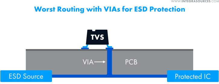
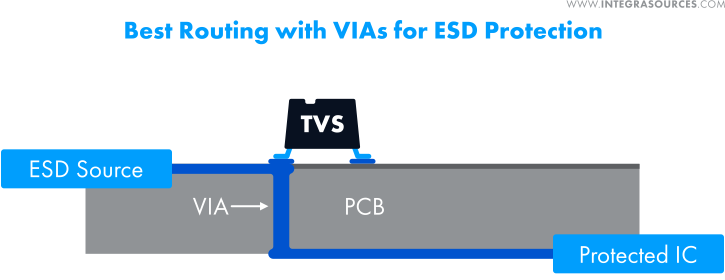
3. Using VIAs properly
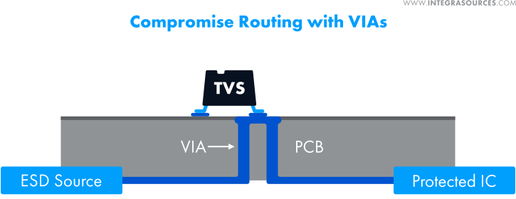
In multilayer PCBs, VIAs can work as needless traces with parasitic inductances. In the picture below, the ESD Source and the Protected IC are located on the same layer, while the TVS is on another layer. Here, the VIA works as L2, causing the ESD current to branch between the TVS and the IC. That’s why this layout must be avoided.
Ideally, the ESD Source and the TVS should be placed on the same layer, like in the picture below. This way, the ESD current goes to the TVS protection pin before moving through the VIA to the protected circuit.
In this particular PCB design, the ESD Source (USB connector) has two traces on two different layers. Placing them on the same level as the TVS wasn’t possible. However, the team used an acceptable layout design.
We had a reverse situation: the TVS and the Protected IC are placed on the same layer, but the ESD Sources (two traces coming from the USB) are on different layers. Despite that, it’s an example of the proper use of VIAs, as the TVS protection pin will receive the ESD current before letting it flow to the IC.

If the ideal layout cannot be implemented, an acceptable compromise is to force the ESD current to the TVS in the following way:
Conclusion
An electrostatic discharge event can be caused by seemingly harmless actions. Nevertheless, ESD damage can be very serious. In a best-case scenario, one will have to reboot the device. But in the worst case, the event will lead to a catastrophic failure.
Electronics designers use multiple methods of protecting devices from ESD.
First of all, using antistatic tools and equipment guarantees protection when engineers work on the device. These tools are designed to discharge static electricity to ground and not let electrostatic charges accumulate on the surfaces within the working area.
To protect the device during operation, designers use various ESD protection devices. The most commonly used components are TVS diodes. These devices shunt the electrostatic current to ground whenever the input voltage reaches a certain threshold.
And finally, one can limit the effects of the event with proper PCB design techniques. The goal here is to reduce the impedance between the ESD Source and the TVS diode array as much as possible to avoid the ESD current flowing to the protected integrated circuit.
Proper protection against electrostatic discharge events improves the reliability of devices, thus saving thousands of dollars for companies offering new products. If you are looking for a professional team for your development projects, you can count on Integra Sources. Contact us directly to discuss your project idea or problem.
Timur Yuldashev
IT Writer, PhD in Philological Sciences
Andrey Solovev
Chief Technology Officer, PhD in Physics and Mathematics
Related
materials
Cases


A Ready-To-Fly Quadcopter
The quadcopter is 10x10 centimeters in size. It can be controlled over a Sony PlayStation 2 gamepad or any other...
LEARN MORE 
LEARN MORE
Infographics

Electronics Prototyping in Infographics
Any product development starts with designing a prototype. Although the first iterations are far from the final product, it’s an...
LEARN MORE
LEARN MORE
Articles

What Makes Electronics Prototyping so Important for Successful Product Development?
Electronics prototyping answers a range of crucial questions, such as how to solve a particular engineering problem, how to do...
LEARN MORE
LEARN MORE